For SEM beam energy greater than 3 keV, electrons penetrate the surface of the sample. The difference between number of electrons that enter the sample and the number that exit as ground current or emitted electrons cause the sample to be electrically charged. This phenomenon can be used to locate opens in metal lines or via chains. No external power supplies are required since the electron beam biases the sample. Conductive coatings should not be used.
Theory
As a rule of thumb, the primary beam of a SEM penetrates IC materials about 1000 Å per 1000 eV of beam energy. A 10 keV beam will penetrate about 1 micron. An isolated conductor covered with one micron of passivation will become negatively charged due to the build up of electrons trapped from the beam. Grounded conductors remain neutral as electrons flow away.
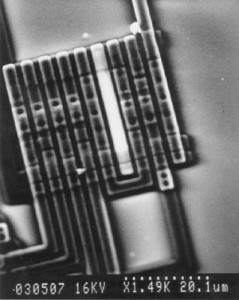
Fig. 1 shows one unused strip of metal 2 which has been charged by the electron beam. Similar dramatic results could be observed at beam energies between 10 and 20 keV. At lower energy, the beam does not reach the metal line. At higher energy, the beam penetrates through the metal line to grounded layers beneath.

Figure (1) Metal is 1 micron thick and is covered by 1 micron of passivation. The isolated strip of metal is bright because secondary electrons are repelled from the sample toward the detector by negative trapped charge.
Equipment
Internal mechanical microprobes are available for most SEM models. Contact Accelerated Analysis for more information.
Example
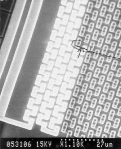
A test structure containing 5000 metal 1 / metal 2 vias was found to be electrically open. The wafer was examined by passive voltage contrast in a SEM. The location of the discontinuity is shown in Fig. 2. This photo isolates the failing via to one of two possible sites. The next step in the analysis will be to examine the site of failure. A cross section by mechanical polishing or by FIB is now a possible next step.

Figure (2) The floating end of the via chain is bright because of trapped negative charge. The remainder of the chain is neutral, and thus darker, because excess electrons are shunted to ground.
Accelerated Analysis
PMB Q-310
Half Moon Bay, CA 94019
DavidBurgess@AcceleratedAnalysis.com
Phone: 650-867-8443 | Fax: 408-241-0547

